Looking back, my fourth semester project was kind of a stretch in terms of useability. We have to create something that we think is exciting, but also fullfills the study regulations. Sometimes, very funky projects is the outcome of that.
A little background before telling you about the project. AAU has multiple student run organization that builds different stuff or simply meet up to discuss different topics. I was very inspired by AAUSAT, which is a project to launch nanosatelittes build by students. Also AAU Racing, that builds and races a Formula type car. However I wanted a project that was grounded and actually had a posibillity to make a scientific and environmental contribution. Since AAUSAT was launching stuff into space and AAU Racing was still using fossil fuels, none of them intrigued me enough to join.
So I had to start my own project. This was where I came up with the idea of a vertical farming system on AAU. The project was to be run by students and would include a vertical farm in a 40 foot shipping container on campus. I contacted my semester coordinator to ask him how I should proceed.
First I was told to make a presentation and a rough budget. Then he got me a meeting with the head of the institute. He liked the idea. They then got me a meeting with a mega-project coordinator and the pro-dean of the university. They also really liked the idea and it actually got approved for funding. Great, then COVID came. Everyone got sent home for the better part of a year and the project got hung up in bureacracy. So the project never got if it’s feet. But I am still glad that I did it and I proved a lot to myself about what is possible as long as you step up. It really showed me that if you want something, you have to work for it and actually ask for what you want.
Anyway, back to the project.
So I had this massive project. For the semester project, all of the adminstration mentioned above thought it would be great if it could be used to get some other students involved. Of course I agreed with that. So I made a project proposal of doing a somewhat scaled version of the system. This scaled version was to be placed in the institute canteen for people to see and ask questions about. My project group and I made a 3D model of the system that you can see below.
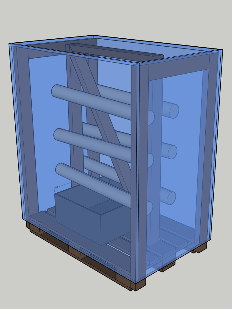
The system was designed to be an NFT system, where water runs down through the pipes into a resovoir at the bottom. The water would then be pumped back up and recirculated. It would be placed on an EUR pallet for easy transportation.
Now since the topic of the semester was Digital Design, we couldn’t just make a simpel Arduino control of the system. We had courses on Real-Time Systems and Design of Digital Systems using PSoC’s and FPGA’s. So we decided that we would make two seperate systems. One main unit that would be implemented on an FPGA (basically a CPU) and a another system that would handle all the interfaces to the different sensors. The latter would be implemented on a Cypress PSoC. The two systems would then communicate using a UART interface that was already implemented on the PSoC, but would be a custom implementation in the FPGA.
The different sensors and simpel system diagram can be seen in the figure below.
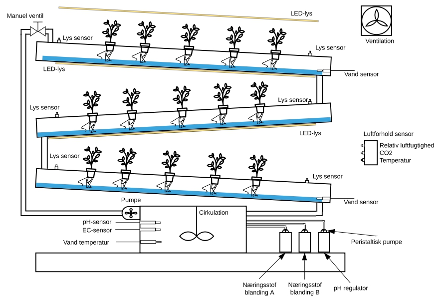
The following sensors and actuators were used in the system:
- pH-sensor
- EC-sensor
- Water temperature sensor
- Water sensor
- Air conditioning sensor
- Light sensor
- LED Grow lights
- Circulation pump
- Water Pump
- Ventilation Fan
All sensors and actuators were controlled by the PSoC.
Since the semester was focused around digital design, we spent a lot of report pages explaining how different interfaces such as I2C, SPI and UART works. But we also got to dive deeper in how ADC’s work and the different architectures used in most IC’s today.
We made a Real-Time system analysis using CODARTS, which was probably a little bit overkill think back at it. The system did not really need to work real-time and we could have easily left it out. However it was a part of the course we were taught, so we included it to show that we had understood it.
We chose to run a FreeRTOS kernel in the PSoC. It was fun to implement and it also meant that we would have the Real-Time aspect of the curricilum covered.
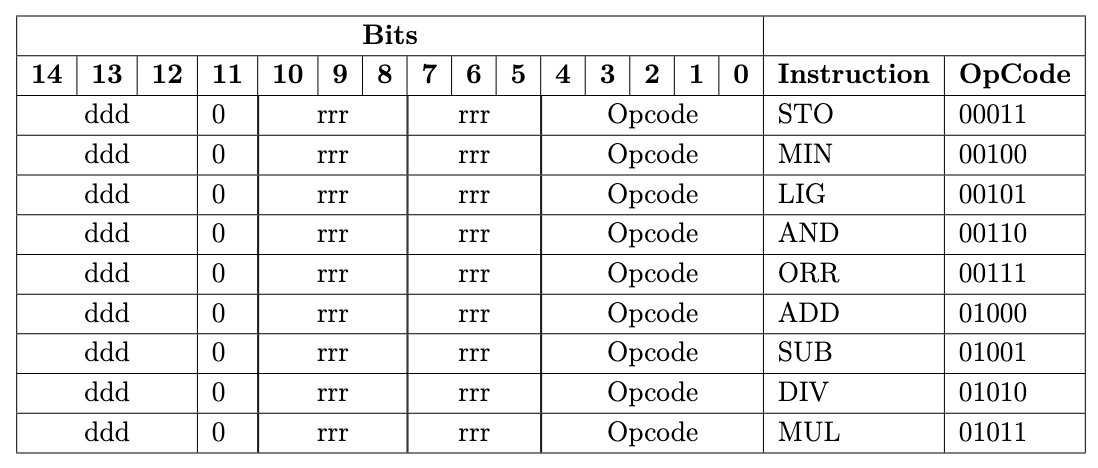
The first thing we did was define and design the Instruction Set Architecture that was gonna be used for the CPU on the FPGA. We designed the ISA from knowing which operations we would need the ALU in the CPU to be able to execute. The resulting operation codes and their functions can be seen in the table below.
| Function | Shortcode | Opcode |
|---|---|---|
| Do nothing | NOP | 00000 |
| SRAM Operations | ||
| Read from SRAM | LAS | 00001 |
| Write to SRAM | SKR | 00010 |
| ALU Operations | ||
| Logic Larger Than | STO | 00011 |
| Logic Smaller Than | MIN | 00100 |
| Equal To | LIG | 00101 |
| Logic AND | AND | 00110 |
| Logic OR | ORR | 00111 |
| Addition | ADD | 01000 |
| Subtraction | SUB | 01001 |
| Division | DIV | 01010 |
| Multiplication | MUL | 01011 |
| Branch Control | ||
| Branch to Instruction | HOP | 01100 |
| Conditional Branch | HOPC | 10001 |
| Perifirals | ||
| UART RX | UAL | 01101 |
| UART TX | UAS | 01110 |
| Show on display | VIS | 01111 |
| UART Conditional branch | HOPUC | 10010 |
The table shows the actual operation described in text, the shortcode which could be used if writing assembly and an opcode in binary, which the assembly code could be translated into. Because of the specific sensors used in this project, it is necessary for the CPU to be designed as a 16-bit machine. This is due to the fact that one of the sensors are outputting 16-bit values. Now we could have designed the CPU to be 8-bit and then just loaded two bytes of data into two 8-bit registers, but that would make the design a little more complicated. Also this would require two ALU operations every time we needed to use that value from the sensor. The instruction set is implemented using the little endian scheme. Meaning instructions are read from right to left. The following abbreviations are used in the design of the codes
| SRAM-adress | = | sssssss |
| Operand register (GPR) | = | rrr |
| Destination register (GPR) | = | ddd |
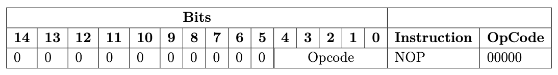
This means that for all instructions in the instruction set, the first five bits from the right will be the opcode. The rest of the bits are then designated to adress registers for the data to either be saved to or loaded from. A simple example of the no operation instruction can be seen below.
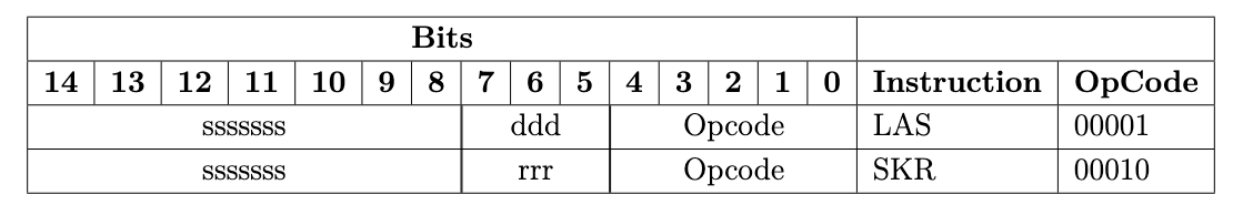
There are also more advanced codes, like the ones used for controlling the SRAM module. These codes needs to have either a destination or an operand register and a SRAM register adress. These codes can be seen below.
Lastly, perhaps the most advanced part of the instruction set are the instructions used for controlling the ALU. This is the module of the design that requires the most amount of operations in order to function. It requires two GPR’s to fetch data from and a single GPR from the destination of the data. The instructions can be seen below
The FPGA part was implemented on a Terrasic DE0-CV and was designed from a microcontroller standpoint. The microarchitecture is designed based on the AVR architecture with one majer difference. The general AVR design uses a Harvard achitecture, meaning the storage for instruction set and data are located in two different parts of the memory. This enables the system to fetch both instructions and data at the same time and thereby potentially making the system faster.
In this project we chose to implement a Von Neumann architecture, where the memory of data and instructions are shared. This is not as elegant, but it’s simpler to implement. The architecture can be seen in the image below.
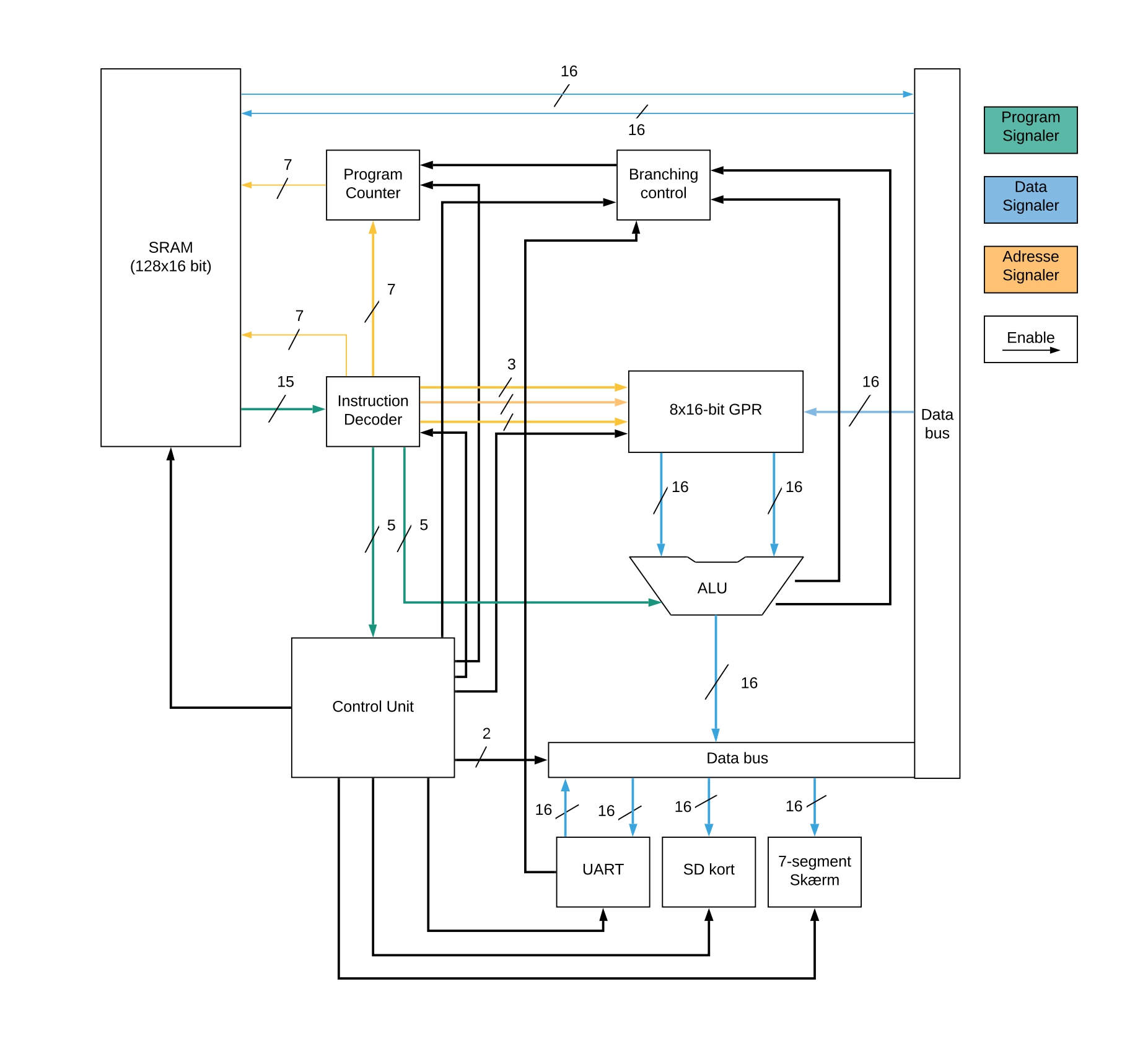
The two most important parts for the control in the architecture is the program counter and the control unit. The program counter outputs the SRAM adress of the current instruction to be executed. There are several inputs to the program counter. One of the more interesting inputs is the branching input. This input makes it possible to skip to a designated command in the program counter.
The control unit takes the opcode and ensures that the correct signals are set across the architecture. By signals I mean the control inputs for all the other elements of the architecture. The control unit is responsible for all of the read and write enable signals to all the registers including the SRAM. To control the control unit itself, a finite state machine has been implemented. The FSM has five states and transitions automatically everytime a rising edge of the clock is observed. The state transition diagram for the FSM can be seen in the figure below.
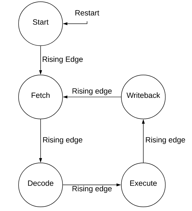
The first state is entered everytime the system is restarted, which is needed in order to send reset signals for all the modules requiring them. Next, is the fetch state. The state is somewhat self-explanatory. It is there in order for the system to fetch the next instruction from memory. In this case, the program counter will send the correct adress for the instruction to the SRAM which will then output the instruction on the next rising edge to the Instruction Decoder.
In the next state, which is the decode state, the Instruction Decoder module will have taken the output from the SRAM and decode it such that the opcode can be passed on to the control unit.
The next state is the execute state, which is the state where all the fun stuff happens. All of the different control signals for the different modules are set in the control unit using the opcode coming from the instruction decoder. In the end, all of the operations that is needed to be carried out in the ALU are carried out and the output is written to the databus.
With the databus being implemented as a register, it is necessary to have one final state in the FSM before completing the cycle. This is the writeback state, where the data located in the databus register is written back into memory and ready for further processing.
The next rising edge will restart the cycle into the fetch state in order to get the next instruction from memory.
The outcome of the project was that we were able to read data of all sensors into the real-time system and transfer them between the CPU and PSoC. We were also able to send new instruction from the CPU to the PSoC.
Because of COVID we never got to see it implemented in the system it was intended to. However we still learned a lot and I consider it one of the most interesting semesters on the Bachelors.